ASSESSMENT BRIEF
| MODULE CODE | MODULE TITLE | |||
| EEEE3083 | Power Electronic applications and control | |||
| ASSESSMENT NAME | ASSESSMENT TYPE | WEIGHT | ||
| Coursework 1 | Individual Report | 30.0 | ||
| ASSESSMENT TITLE | METHOD OF SUBMISSION/ DELIVERY | |||
| Average Modelling Design and Switching Model Verification of a
Full Bridge Inverter |
Moodle | |||
| ASSESSMENT DATE / SUBMISSION DEADLINE | FEEDBACK DUE | |||
| Monday, 17th November 2025 3:00:00pm | Monday, 8th December 2025 | |||
Struggling with Your EEEE3083 Power Electronic Aplications and Control Coursework?
MARKING AND FEEDBACK DETAILS
☒ Marked anonymously
☐ Not marked anonymously
As this assignment is to be marked anonymously, please ensure that your submission does not include any identifying information.
MODULE LEARNING OUTCOMES ASSESSED
☐ 1 Describe and analyse the operation of a range of practical power electronic circuits and their applications
☐ 2 Apply basic average techniques to model a range of practical power electronic circuits
☐ 3 Apply basic design calculations for a range of practical power electronic circuits and their applications
☐ 4 Describe and analyse typical control tasks in power electronic systems
☐ 5 Describe and apply root locus control techniques to the design of linear continuous and discrete controllers
☒ 6 Assess methods to perform basic average modelling of power electronic circuits and their control design using CAD tools
☐ 7Analyse the performance of power electronic circuits and their control by means of switching models and CAD tools
This assessment also assesses the following AHEP4 outcomes:
C1, C2, C3/M3, C6/M6
KEY SUBMISSION REQUIREMENTS
Document submission must be in docx format.
Simulation files should also be submitted in the form of a .zip and must be separate from the report.
| NO EVIDENCE EC ELIGIBLE? | SPECIFIC RESTRICTIONS ON EC/SUPPORT PLAN EXTENSIONS | ||||
SUPPORT PLAN EXTENSION
If you have an existing support plan and support plan extensions are applicable to this assessment, and you require an extension, please email ee-dlo@exmail.nottingham.ac.uk. Include the module code, assessment name, original deadline (including time), and the requested extension length (usually one working week).
HOW TO GET CLARIFICATION
Please contact David.Dewar1@nottingham.ac.uk either through Teams (Preferred) or Email with any questions. Support sessions are provided Monday 4-5pm each week, open to questions.
AI USAGE POLICY
Permitted Uses of AI:
✓- You may use AI tools to ask questions for clarification if you are confused about a concept, method or requirement.
✓- You may use AI tools to support your understanding of background material (e.g asking to explain definitions, theories or provide analogies to complex concepts.
✓- You may use AI tools to explore ideas or approaches informally, provided you then write and develop your own work independently.
✓- You may use AI tools to check your own understanding (e.g., asking “does my reasoning make sense?), but must not be used to generate written content for the submission.
✓- To help debug or interpret error messages when using software (MATLAB / PLECS)
Prohibited Uses of AI:
✗- AI tools must not be used to generate text that appear in the submitted assignment (including answers, explanations, or report sections).
✗- AI tools must not be used to create figures, diagrams or graphics for submission.
✗- AI tools must not be used to produce worked solutions to the final answer that are then submitted directly.
✗- Copying, paraphrasing or presenting AI-generated material content as your own is strictly prohibited.
Academic Misconduct:
Any breach of the above rules will be treated as academic misconduct and will be referred to the
University Academic Misconduct Process
MISCONDUCT INFORMATION
The work submitted must be your own work and must adhere to the University’s Academic Misconduct policy.
Need Expert Help for Your University of Nottingham EEEE3083 Coursework?
Power Electronic Applications and Control Coursework 1: Average Modelling Design and Switching Model Verification of a Full-Bridge Inverter
Introduction
This coursework introduces you to the design and verification of a full-bridge inverter, a core building block in power electronics. The aim is to give you practical insights into how engineers approach converter design, from first principles to full system verification.
The assignment is split into two parts. In the first part you will develop and test an average model of the inverter to design filters and controllers in a simplified, numerical framework. In the second part you will then move you design into a switching model to verify that your design performs as expected in realistic conditions.
Your role is to act as a design engineer:
- Apply knowledge from the module to meet the given specification.
- Document your design choices clearly and logically.
- Communicate results for both technical and non-technical stakeholders.
Your report should therefore not only present results, but also explain your design methodology, justify key decisions, and reflect on observed behaviours. Where appropriate, you should support your reasoning and observations with references to literature.
The page limit for this report is strictly 25 pages (excl. Title Page / Contents Page / Appendices). Please note material documented in the appendices will not be marked.
Learning Outcomes
By completing this coursework, you will be able to:
- Develop an average model of a single-phase inverter and use it to design filters and controllers.
- Translate average-model results into a switching-level implementation and verify performance in simulation.
- Analyse the effects of passive components and controller parameters on inverter behaviour.
- Present technical results in a professional report format suitable for engineering and non-technical audiences.
Part 1 : Average Modelling
In the first stage, you will design and test an average model of a single-phase H-Bridge inverter (Figure 1). Average modelling ignores the switching dynamics and instead represents the converter in terms of average quantities over a switching period. This simplifies analysis, allowing you to design and verify filters and controllers before moving to more complex switching simulations in Part 2.
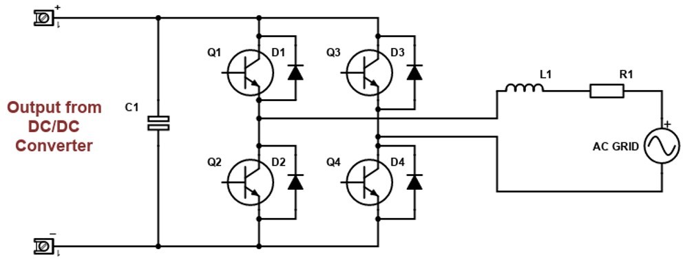
Figure 1- H-Bridge Circuit which CW1 and CW2 will focus on designing.
The target design specification can be found in Table 1. Many of the concepts and methods required for this stage are covered in Inverters Lectures 1 – 3. You can begin the coursework with the knowledge gained from Lecture 1, while Lectures 2 and 3 will provide additional tools to complete the design and verification of the inverter.
Table 1 – Design Specification for Converter to be designed.
| Term | Symbol | Value |
|---|---|---|
| DC Voltage | ( V_{DC} ) | 600V |
| DC Voltage Ripple (peak-peak) | ( Delta V ) | 0.5V |
| AC RMS voltage | ( V_{AC} ) | 240V |
| AC Current ripple (peak-peak) | ( Delta I ) | 0.2A |
| Rated Power | ( P ) | 3kW |
| Inverter Switching Frequency | ( f_{sw} ) | 20kHz |
| Loss in the inductor at rated power | ( P_{LOSS} ) | 0.25%P |
| Settling Time of Inverter (Time to reach 2% reference) | ( t_s ) | 150ms |
Your report must show clear evidence of the following steps:
Core Tasks (for all students)
- Filter Design – Design the output inductor (RL filter) based on the AC current ripple specification
- Passive Effects – Analyse how passive elements influence the circuit variables such as output voltage.
- Average Model in PLECS – Build and Verify the average model of the inverter
- Controller Design (Current Loop) – Derive the transfer functions for the current control loop and design the controller using MATLAB SISOTOOL.
- Controller Verification –
a. Show stable operation at different power levels
b. Demonstrate bi-directional capability (absorbing and delivering power) - DC-Link Capacitor Design – Calculate the required capacitance to achieve the specified voltage ripple.
a. Explain why the average model cannot be used directly for this stage, and why the transfer function must remain in transfer function form. - Voltage Control Loop – Derive the plant transfer function. Draw appropriate block diagrams and design suitable voltage controller.
- Global Verification – Simulate the complete system including both the current and voltage controllers. Show transients in DC voltage and confirm that specifications are met.
Challenge Tasks (for higher marks)
For students aiming to push their design, and critical analysis further, consider:
- Parameter Sensitive Analysis – Vary L and C ±20% and assess the impact on ripple, settling time and stability.
- Stability Margins – Evaluate gain and phase margins using MATLAB Tools.
- Load Variation Test – Analyse the Inverter response with resistive, inductive or variable power factor loads.
- Disturbance Rejection – Apply step changes in DC voltage or load current and evaluate the transient response.
- Cascade Loop Interaction –
a. Explore what happens if the voltage loop is tuned too fast compared to the current loop.
b. Show instability or degraded performance and explain why correct loop hierarchy matters.
Grading Note:
Achieving the Core Tasks to a high standard is sufficient to reach a mark of 80%. The challenge tasks are designed to extend your analysis and demonstrate deeper understanding. Completing them is not required to pass or achieve a high grade, but they can help push your mark further beyond the 80+% threshold.
Part 2: Switching Model Verification
After validating your design with the average model, the next step is to implement it in a switching-level PLECS model. This step verifies that your design performs correctly when applied to a realistic inverter with PWM switching.
The switching simulation should demonstrate that your design choices (filter, controllers, DC-Link capacitance) still meet the specification under non-ideal conditions.
Part 2: Deliverables
Your report must show clear evidence of the following steps:
Core Tasks (for all students)
- Switching Model Construction – Build a full-bridge inverter in PLECS. Use a constant DC Voltage source on inverter inputs. Do not implement your controller at this stage. Instead, apply test voltage demands directly in the PWM modulators and verify that:
a. The average voltage generated by the full-bridge matches the demand.
b. The correct average power is exchanged with the grid.
c. The inductor current ripple is within the expected range. - Controller Integration – Implement your designed current controller into the switching model. Provide an AC current reference and show correct steady-state tracking at different power levels, including power generation and absorption.
- Average vs Switching Comparison – Demonstrate that the average switching voltage matches the demand given to the PWM. Evaluate harmonics of the generated voltage and briefly discuss results.
- Inductor Ripple Verification – Confirm that the inductor current ripple in the switching model matches your design expectation.
- Transient Tests – Apply power steps (0 -> P/2 -> P and back). Show the system response and comment on any discrepancies compared with the average model.
- DC-Link Control – Replace the ideal DC source with a DC-Link Capacitor and Controllable Current Source in parallel. Implement your voltage controller and verify that the DC voltage achieves the desired steady-state value.
- Performance under DC current variation – Increase the DC current from 0 -> Half Rate -> Full Rated. Show the DC voltage response and compare with expected behaviour from the average model. Reflect on what this change in DC current emulates in real systems.
- Ripple Check – At full rated operation, verify that the DC-Link voltage ripple remains within specification.
Challenge Tasks (for higher marks)
For students aiming to push their design, and critical analysis further, consider:
- Hamonic Analysis – Quantify the Total Harmonic Distortion of the inverter output voltage and current. Compare your results against relevant industrial standards (i.e IEEE 519 for current harmonics or IEEE 1547 for inverter interconnection specifications) Comment whether the design would meet compliance requirements and what modifications might be needed if not.
- Controller Robustness – Re-run the transients with deliberately mistuned PI parameters (too high / too low gains) and show the impact on ripple and stability. What could this mean in realistic situations?
- Grid Disturbance Test – Apply a temporary sag or swell (short-term deviation of the grid RMS voltage from its nominal value) to the AC grid source in your model. Evaluate the inverter’s response, and explain what kind of real-world situations this test is emulating.
Grading Note:
Achieving the Core Tasks to a high standard is sufficient to reach a mark of 80%. The challenge tasks are designed to extend your analysis and demonstrate deeper understanding. Completing them is not required to pass or achieve a high grade, but they can help push your mark further beyond the 80+% threshold.
Tips for the Assignment:
- Start Early – Do not leave this assignment until the final week before the deadline. Students who delay struggle to finish and receive less support. You are provided with weekly online support sessions (Mondays 16:00 – 17:00) which are timetabled specifically to help you progress – make use of these while working steadily through the coursework.
- Report Style – Write your submission as a professional technical report. Use clear headings, subheadings, figure references and equation labelling. Remember your audience includes both technical and non-technical stakeholders.
- Clarity over Length – A shorter, well-explained design with clear justifications will score higher than a long report filled with raw plots or unstructured notes. Stick to the 25-page limit (excl. title / contents / appendices) Please note, any materials in the appendices will not be marked.
- Figures and Tables – Ensure all plots and diagrams are clearly labelled, with readable text when printed. Highlight key results directly on the plots (e.g ripple, settling time, rated power) so the reader does not have to search.
- Limitations – Always comment on the limitations of your model or controller design (e.g ideal sources, no thermal effects, limited bandwidth). Acknowledging these strengthens your report.
- Limitations – Begin Part 1 as soon as possible (you can start once you have covered Inverters Lecture 1). Aim to finish part 1 early so you have enough time for the switching model in Part 2.
- Challenge Tasks – Completing the core tasks to a high standard is enough for First / Distinction Level marks (80+). Challenge tasks are optional extensions to push your work and knowledge further.
Can’t Complete Your EEEE3083 Assessment Coursework 1 Individual Report on Time?
The post EEEE3083 Power Electronic Aplications and Control Assessment Coursework 1 Individual Report | University of Nottingham appeared first on Students Assignment Help UK.